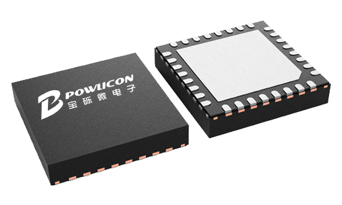

LYF62001是一款集成快速充电协议的高效、同步双向升降压SOC 样品订购
一、产品详情
1、产品特征:
-
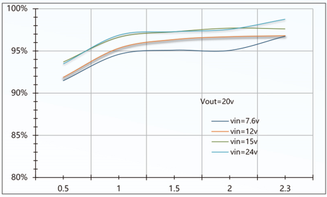
输入电压范围:3.0V-32V
-
输出电压范围:2.0V-30V
-
可编程开关峰值电流:20A
-
开关频率:150KHz/300KHz
-
集成全快充协议、buck-boost充放电控制器、电源路径管理
-
支持A+C应用、集成I²C通信
-
电池类型3V-4.5V可每10mV递增设置,支持1-6串电池
-
适配器防拉死电压VINREG可每10mV递增编辑
-
输入输出电流限制可每10mA递增编辑
-
输出电压可每10mV递增编辑
-
支持欠压、过压、过流、短路、温度等保护
-
集成LDO
-
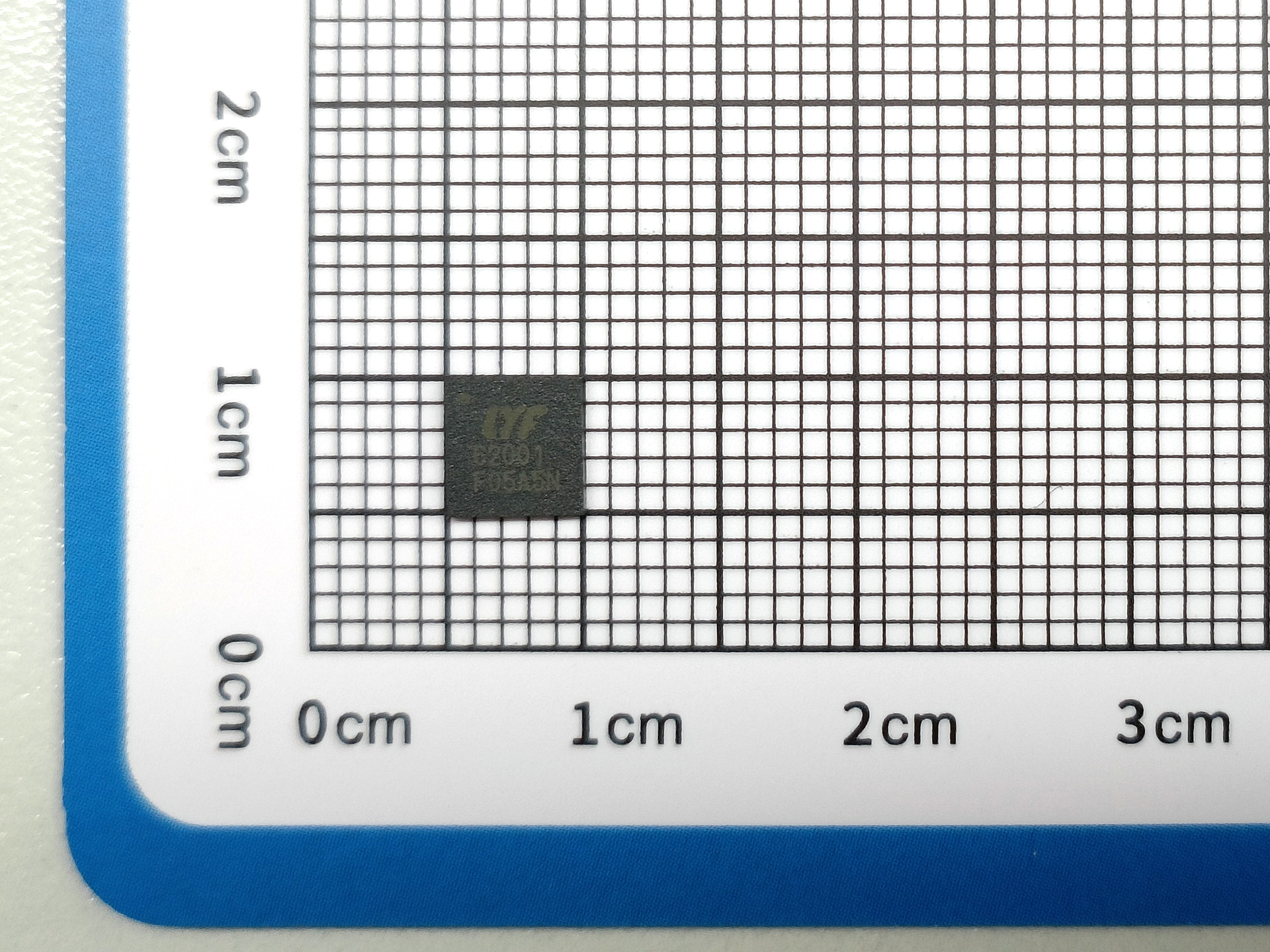
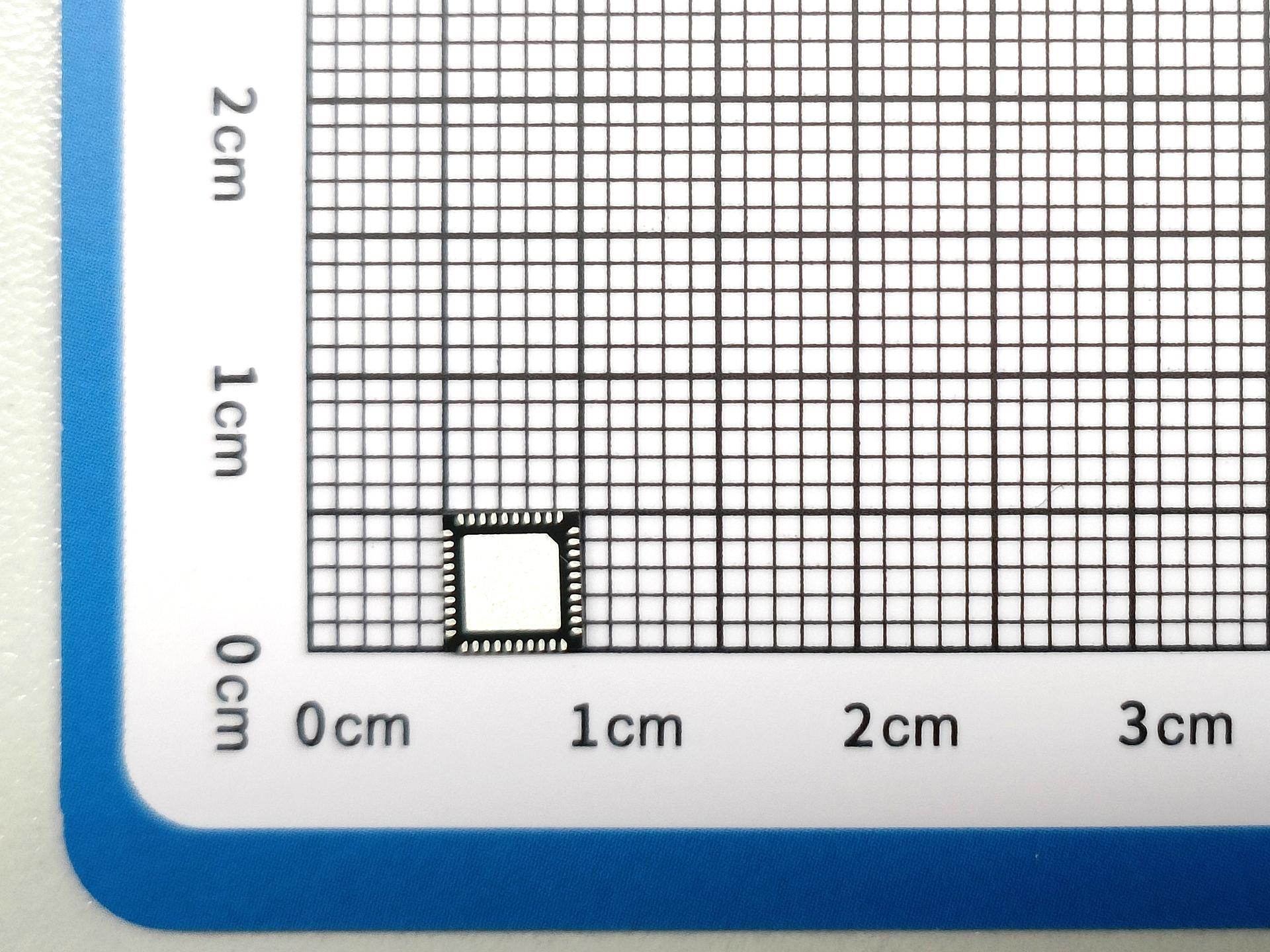
封装:QFN5x5-40
2、应用原理图:
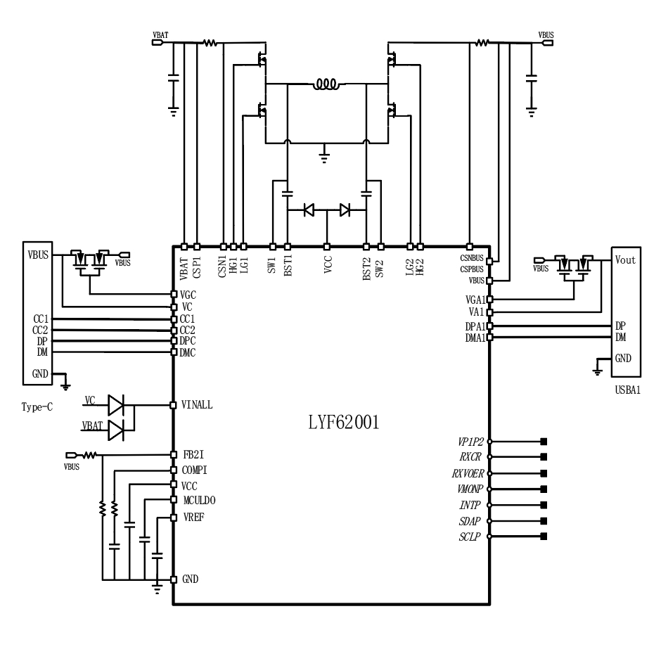
LYF62001应用原理图
3、产品描述
LYF62001 is a high efficiency, synchronous bi-directional buck-boost charger with integrated fast charge protocols. It is a comprehensive and flexible buck-boost charger platform designed for most of fast charging applications with type-C port and PD protocol. It can be programmed to buck charging, boost charging or buck-boost charging. LYF62001 provides I2C interface to communicate with MCU, provides high voltage sensing for battery and BUS terminals, accurate rail-rail current sensing for battery current, BUS current and USB ports currents. It also provides high voltage blocking for CC1, CC2, DP, DM communication signals for all of the USB ports. LYF62001 can work with a general MCU to provide a complete, powerful and flexible buck-boost charging system for all kinds of fast charge application such as power bank, battery packs, or portable energy cubic etc.
In charging mode, it steps up or down the input voltage to effectively charge the batteries. LYF62001 supports trickle charging, constant current (CC) charging and constant voltage (CV) charging management. The charging current and charging voltage can be programmed by two 12-bit DAC converters.
The LYF62001 features I2C interface, so the user can easily control the charging/discharging mode, and program charging current, charging voltage, output voltage, and output current limits through I2C. It also monitors the status of USB ports and provides two NMOS gate drivers to control the power path independently. User can also use I2C to monitor the status of DC-DC, even the whole system.
LYF62001 also provides VMON pin, through which the MCU can monitor VBUS, VBAT voltage, IBUS, IBAT current and the current of each port in real time. All these features simplify the system design and reduce BOM cost for any charging system.The LYF62001 supports under voltage protection, over voltage protection, over current protection, short circuit protection and over temperature protections to ensure system safety under different abnormal conditions.
4、典型应用场景
-
充电宝
-
移动储能
-
电池包
-
移动设备(如电动工具、筋膜枪、移动家电等)
-
应急启动电源
-
智能USB插座
5、封装信息
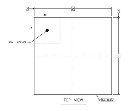
LYF62001顶视图
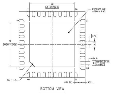
LYF62001背视图
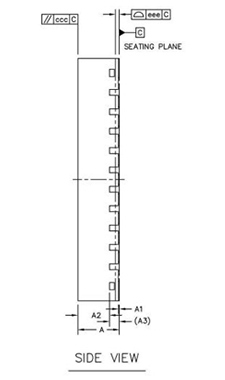
LYF62001侧视图
6、管脚定义和功能描述
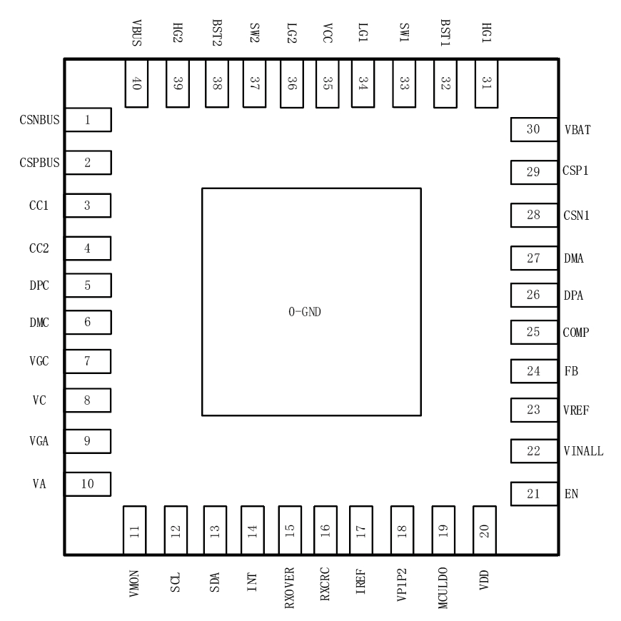
LYF62001管脚定义图
管脚功能描述
| 序号 | 名称 | 描述 |
|---|---|---|
| 1 | CSNBUS | Negative input of a current sense amplifier. Connect to one terminal of the current sense resistor. |
| 2 | CSPBUS | Positive input of a current sense amplifier. Connect to one terminal of the current sense resistor. |
| 3 | CC1 | Configuration Channel 1 for C port |
| 4 | CC2 | Configuration Channel 2 for C port |
| 5 | DPC | D+ signal for C port |
| 6 | DMC | D- signal for C port |
| 7 | VGC | NMOS gate driver to control the external NMOS of C port |
| 8 | VC | Used to sense the voltage of C port. |
| 9 | VGA | NMOS gate driver to control the external NMOS of A port |
| 10 | VA | Used to sense the voltage of A port. |
| 11 | VMON | Used to detect VBUS/VBAT voltage, IBUS/IBAT current, and the voltage drop of cut-off MOS for A/C ports. Connect this pin to MCU with a RC filter. |
| 12 | SCL | I2C clock line. Connect with a pull up resistor (typical 10kΩ). Connect to MCU |
| 13 | SDA | I2C data line. Connect with a pull up resistor (typical 10kΩ). Connect to MCU |
| 14 | INT | Open drain output for interrupt signal. Connect to MCU |
| 15 | RXOVER | Connect this pin to MCU |
| 16 | RXCRC | Connect this pin to MCU |
| 17 | IREF | Reference voltage for input and output current limiting loop. |
| 18 | VP1P2 | 1.2V power supply. |
| 19 | MCULDO | 3.3V voltage output for MCU |
| 20 | VDD | Output of internal 5V linear regulator. Connect a 1μF capacitor from VDD pin to GND as close to the IC as possible. |
| 21 | EN | Logic High will enable the converter. Logic Low will disable the whole LYF62001. EN is pulled high internally by a 5000kΩ resistor. |
| 22 | VINALL | Power supply to the IC. Connect to power rails with low voltage schottky diodes. Place a 1μF capacitor from this pin to GND as close to the IC as possible. |
| 23 | VREF | Reference voltage for voltage control loop |
| 24 | FB | VBUS voltage feedback. |
| 25 | COMP | Error amplifier output and input to the PWM comparator. Connect frequency compensation components to this pin. |
| 26 | DPA | D+ signal for A port |
| 27 | DMA | D- signal for A port |
| 28 | CSN1 | Negative input of a current sense amplifier. Connect to one terminal of the current sense resistor in the VBAT side. |
| 29 | CSP1 | Positive input of a current sense amplifier. Connect to one terminal of the current sense resistor in the VBAT side. |
| 30 | VBAT | Battery voltage or Input voltage. Place a 1μF capacitor from this pin to GND as close to the IC as possible. |
| 31 | HG1 | High side gate driver of switch MOS |
| 32 | BST1 | Boot-Strap pin Connect a 0.1µF or greater capacitor between SW and BST to power the high side gate driver. |
| 33 | SW1 | Power Switching pin. Connect this pin to the switching node of inductor. |
| 34 | LG1 | Low side gate driver of switch MOS |
| 35 | VCC | Power supply for high side and low side driver |
| 36 | LG2 | Low side gate driver of switch MOS |
| 37 | SW2 | Power Switching pin. Connect this pin to the switching node of inductor. |
| 38 | BST2 | Boot-Strap pin Connect a 0.1µF or greater capacitor between SW and BST to power the high side gate driver. |
| 39 | HG2 | High side gate driver of switch MOS. |
| 40 | VBUS | Power node of the charger. |
二、技术文档
| 类型 | 标题 | 上传时间 | 文档下载 |
| 产品规格书(英文) | LYF62001_Datasheet_en_R1.0 | 2025/04/09 | PDF下载 |
| 设计指南 | LYF62001 PCB设计指南 | 2025/04/09 | PDF下载 |
三、应用方案
| 序号 | 标题 |
| 1 |
30-100W电动工具充电方案
30-100W电动工具充电方案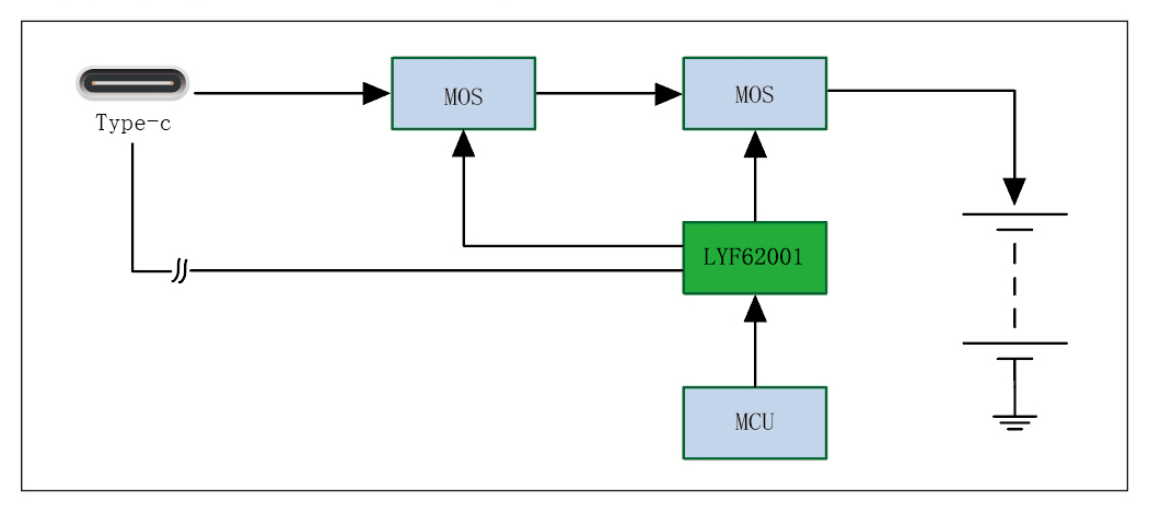
|
| 2 |
储能电源应用方案
储能电源应用方案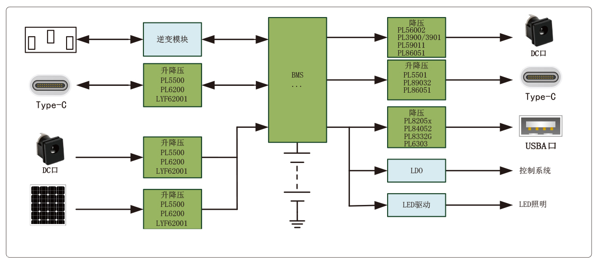
|
| 3 |
充电宝A+C应用方案
充电宝A+C应用方案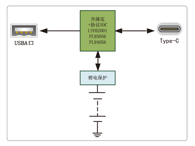
|


 立创商城
立创商城
 世强硬创平台